Time:2025-11-15 Views:1 source:News

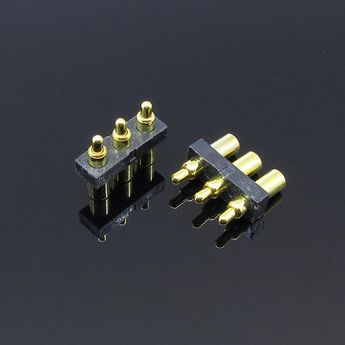
Pogo Pin electronic assembly probes are specialized contact components designed to support the intricate processes of electronic device assembly, including PCB assembly, component bonding, and final device integration. Unlike manufacturing probes focused on post-assembly testing, these probes play an active role during the assembly process—providing temporary electrical connectivity for tasks such as in-circuit programming (ICP) of microcontrollers, voltage supply for active alignment of optical components (e.g., camera modules), and real-time monitoring of soldering temperatures. Their design prioritizes ease of integration into assembly fixtures, compatibility with small form factors, and reliable contact during dynamic assembly steps.
The technical design of electronic assembly probes emphasizes integration and adaptability. They feature a compact, low-profile structure (with heights as small as 3mm) to fit into tight assembly fixtures, especially for miniaturized devices like smartwatches or IoT sensors. The probe pins are made of durable, high-conductivity materials (e.g., nickel-plated brass or gold-plated beryllium copper) that can withstand the mechanical stress of repeated insertion into assembly jigs, while maintaining low contact resistance (less than 40 milliohms) for stable power and data transmission. Many models include a “self-centering tip” design (e.g., rounded or chamfered tips) that ensures accurate alignment with PCB pads or component pins, even if the fixture has minor tolerances—critical for preventing misalignment during high-speed assembly.
In electronic assembly workflows, these probes enable key process steps that would be impossible with traditional methods. For in-circuit programming, Pogo Pin arrays mounted on programming fixtures make temporary contact with the PCB’s test points, allowing the microcontroller to be programmed with firmware before the device is fully enclosed—eliminating the need for post-assembly programming ports and reducing device size. For active alignment of optical components (e.g., aligning a smartphone’s camera lens with its image sensor), probes supply power to the sensor while transmitting real-time image data to a monitoring system—engineers can adjust the lens position until the image quality is optimal, then bond the lens in place. For soldering temperature monitoring, specialized probes with built-in thermocouples measure the temperature of solder joints during reflow soldering, ensuring the temperature stays within the optimal range (e.g., 217°C to 227°C for lead-free solder) and preventing component damage.
Practical advantages of these probes for assembly include improved process efficiency and product quality. Their temporary contact design eliminates the need for permanent test points or connectors, reducing PCB space and device cost—especially important for miniaturized electronics. The real-time data transmission capability allows for immediate process adjustments, such as correcting lens alignment or adjusting soldering temperatures, reducing the number of defective units. Additionally, their compatibility with automated assembly systems enables seamless integration into robotic assembly lines, increasing production speed while maintaining precision. For electronics manufacturers, Pogo Pin electronic assembly probes are transformative tools that streamline assembly processes, reduce costs, and ensure the reliability of complex electronic devices.
Read recommendations:
Advantages of Single-Pin Spring Pogo Pins in Medical Devices
Testing Methods for the Insertion and Extraction Life of Pogo Pins