


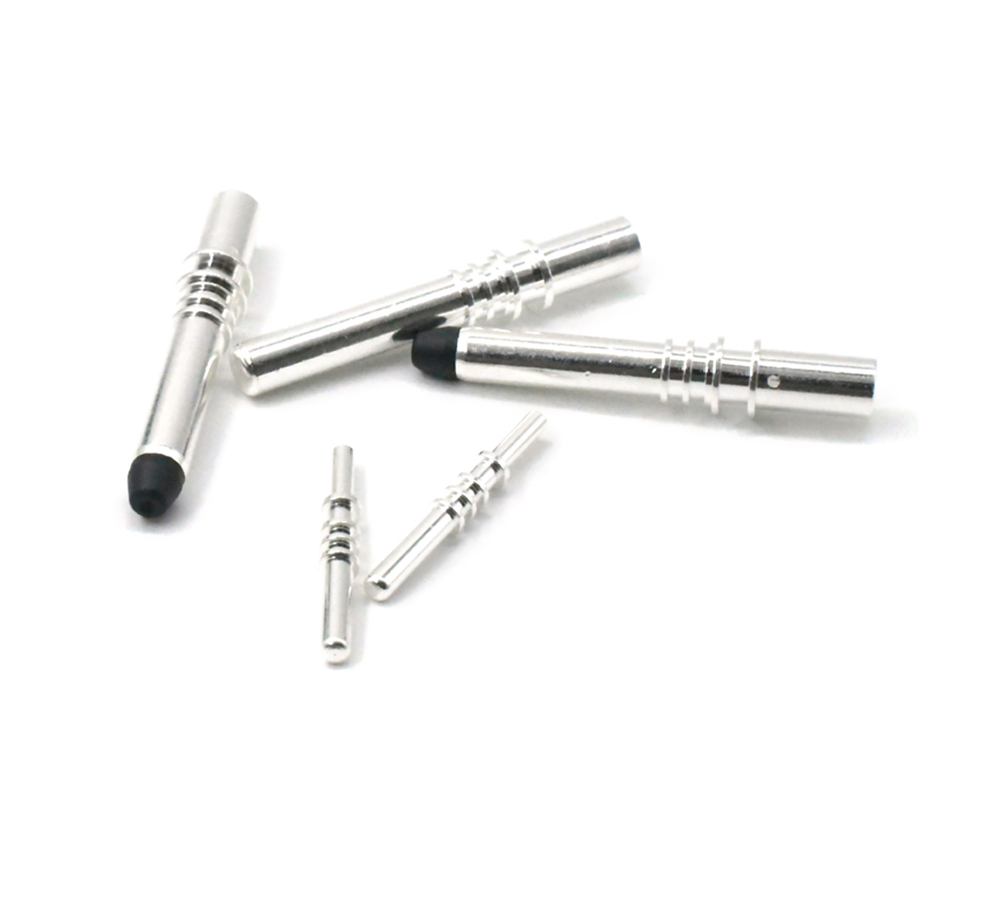
The Pogo Pin connector footprint refers to the physical layout and dimensions of the Pogo Pin connector on a printed circuit board (PCB). It encompasses the size, shape, and spacing of the pads where the Pogo Pins are mounted, as well as any additional features such as mounting holes or alignment marks. A well - designed Pogo Pin connector footprint is crucial for ensuring proper mechanical and electrical connections, as well as for facilitating the manufacturing and assembly processes.
The size of the Pogo Pin connector footprint is determined by several factors, including the size of the Pogo Pins themselves, the required contact area for electrical conductivity, and the mechanical support needed. Larger Pogo Pins may require larger pads to ensure a secure soldering connection and sufficient electrical contact. The spacing between the pads is also an important consideration. It needs to be wide enough to prevent short circuits between adjacent pins, while also being narrow enough to fit within the available space on the PCB. In high - density applications, where a large number of Pogo Pins are used, precise control of the pad spacing is essential to achieve a compact and reliable design.
The shape of the Pogo Pin connector footprint can vary depending on the design requirements. Common shapes include rectangular, circular, and custom - designed shapes to fit specific mechanical or electrical needs. The shape of the pads can also be optimized to improve the soldering process. For example, rounded pads can reduce the risk of solder bridging between adjacent pins, while square or rectangular pads may provide better mechanical stability.
In addition to the pads for the Pogo Pins, the connector footprint may also include other features. Mounting holes are often included to provide mechanical support and secure the connector to the PCB. These holes need to be accurately positioned to ensure proper alignment of the Pogo Pins. Alignment marks, such as fiducial marks or alignment holes, can also be added to assist with the assembly process. These marks help the automated assembly equipment accurately position the Pogo Pin connector on the PCB, reducing the risk of misalignment and improving the overall assembly yield.
The design of the Pogo Pin connector footprint also needs to take into account the manufacturing process. The pad layout should be compatible with the soldering method used, whether it is reflow soldering, wave soldering, or hand soldering. For reflow soldering, the pads need to be designed to ensure proper wetting of the solder paste and even heat distribution during the soldering process. In addition, the footprint should be designed to minimize the risk of solder defects, such as voids or cold joints.
A well - defined Pogo Pin connector footprint is essential for the successful integration of Pogo Pin connectors into PCBs. It affects the electrical performance, mechanical stability, and manufacturing feasibility of the PCB assembly. Designers need to carefully consider all the relevant factors and follow industry standards and best practices to create an optimal Pogo Pin connector footprint that meets the requirements of the specific application.
Read recommendations:
New supplier of CCS1 to Tesla adapter
Customized Pogo Pin connector price


159-2067-7287 Mr. Wan

0769-86006029

No. 5, Zhenrong Road, Wusha, Chang'an Town, Dongguan City
 Whatapp
CopyRight © 2024 Dongguan Yongtan New Energy Co., Ltd. All Rights Reserved


 CN
CN
 Home >