Time:2025-11-21 Views:1 source:News

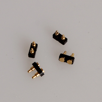
A Pogopin PCB probe card is a high-precision testing component designed to establish reliable electrical connections between test equipment and printed circuit boards (PCBs) during manufacturing or quality inspection processes. Unlike traditional rigid probe cards, it integrates Pogopin (spring-loaded pin) technology—featuring small, retractable pins with spring mechanisms—to ensure consistent contact pressure, low contact resistance, and excellent durability, making it ideal for high-density PCB testing scenarios such as semiconductor packaging, consumer electronics PCBs, and automotive electronic control unit (ECU) boards.
The core structure of a Pogopin PCB probe card consists of Pogopin pin arrays, insulating substrate, wiring layer, and interface connector. Pogopin pin arrays are the key functional part: each pin is typically 0.1mm to 0.5mm in diameter, with a spring inside that provides 10g to 50g of contact pressure—ensuring firm contact with PCB pads even if there are minor height variations (up to ±0.1mm) on the PCB surface. The pins are usually made of high-conductivity materials like beryllium copper (BeCu) or phosphor bronze, with a plating layer of gold (Au) or palladium-nickel (Pd-Ni) to reduce contact resistance (typically ≤50mΩ) and resist corrosion. The insulating substrate, often made of high-temperature-resistant materials like ceramic (Al₂O₃) or polyimide (PI), arranges the Pogopin pins in precise arrays (matching the PCB’s pad layout) with positional accuracy up to ±0.01mm—critical for testing high-density PCBs with pad pitches as small as 0.3mm. The wiring layer (etched copper traces on the substrate) connects each Pogopin pin to the interface connector, which links the probe card to test equipment (e.g., automatic test equipment, ATE) for signal transmission.
Technical advantages of Pogopin PCB probe cards include high contact reliability, strong adaptability to PCB variations, and long service life. High contact reliability is achieved through the spring-loaded design: the pins retract slightly when in contact with the PCB, maintaining stable pressure even if the PCB has warpage (common in thin PCBs) or uneven pad heights. This avoids intermittent connections that could lead to false test results. Strong adaptability is reflected in its compatibility with various PCB types—from single-layer to multi-layer PCBs, and from rigid PCBs to flexible PCBs (FPCs). For flexible PCBs, the gentle contact pressure of Pogopin pins prevents damage to the fragile FPC surface. Long service life is a standout feature: each Pogopin pin can withstand 100,000 to 1,000,000 contact cycles (far more than traditional rigid probes’ 10,000 cycles) due to the wear-resistant plating and robust spring design, reducing replacement costs for manufacturers.
In practical applications, Pogopin PCB probe cards are widely used in electronics manufacturing. In semiconductor packaging testing (e.g., IC chips like microcontrollers), the probe card connects the ATE to the chip’s bonding pads on the PCB, testing electrical parameters such as voltage, current, and signal integrity to identify defective chips. In consumer electronics (e.g., smartphone PCBs), it tests components like touchscreen controllers and camera modules, ensuring each PCB meets performance standards before assembly. In automotive electronics, it inspects ECU PCBs for functions like engine control and safety systems, where reliable testing is critical for vehicle safety. For manufacturers seeking high-precision, durable PCB testing solutions, Pogopin PCB probe cards are an indispensable component.
Read recommendations:
Efficient production of Magnetic PogoPin for Portable Power Supplies